
Extreme ultraviolet lithography (EUVL, also known simply as EUV) is a new technology used in the semiconductor industry for manufacturing integrated circuits...
119 KB (13,917 words) - 01:52, 3 September 2024

ASML Holding (redirect from ASM Lithography)
semiconductor industry and the sole supplier in the world of extreme ultraviolet lithography (EUV) photolithography machines that are required to manufacture...
41 KB (3,392 words) - 18:21, 21 August 2024

the terms. The main uses of extreme ultraviolet radiation are photoelectron spectroscopy, solar imaging, and lithography. In air, EUV is the most highly...
13 KB (1,518 words) - 00:56, 30 May 2024
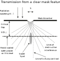
Photolithography (redirect from Optical lithography)
including ultraviolet lithography, deep ultraviolet lithography, extreme ultraviolet lithography (EUVL), and X-ray lithography. The wavelength of light...
57 KB (6,382 words) - 17:25, 4 September 2024

wavelength bands in the UV spectrum. 13.5 nm: Extreme ultraviolet lithography 30–200 nm: Photoionization, ultraviolet photoelectron spectroscopy, standard integrated...
114 KB (12,501 words) - 04:12, 21 August 2024
generate secondary electrons as in the cases of extreme ultraviolet lithography and electron beam lithography. While the fine pattern definition is due principally...
12 KB (1,623 words) - 17:49, 28 December 2022
laser lithography has enabled transistor feature sizes to shrink from 800 nanometers in 1990 to 7 nanometers in 2018. Extreme ultraviolet lithography machines...
10 KB (1,103 words) - 21:59, 29 July 2024

from 0 to as high as 50 nm (see section New frontiers and extreme ultraviolet lithography). Hence, resist-substrate charging is not repeatable and is...
38 KB (4,736 words) - 09:02, 10 July 2024
Nanolithography (category Lithography (microfabrication))
set include multiphoton lithography, X-Ray lithography, light coupling nanolithography (LCM), and extreme ultraviolet lithography (EUVL). This last technique...
16 KB (1,682 words) - 09:17, 28 May 2024
3 nm process (category International Technology Roadmap for Semiconductors lithography nodes)
they had taped out 3nm test chips, using extreme ultraviolet lithography (EUV) and 193 nm immersion lithography. In early 2019, Samsung presented plans...
43 KB (3,590 words) - 15:21, 27 August 2024